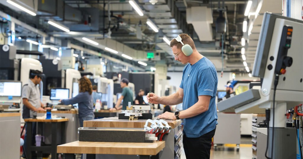
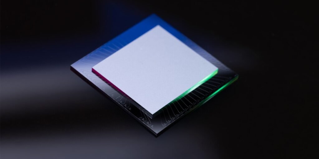
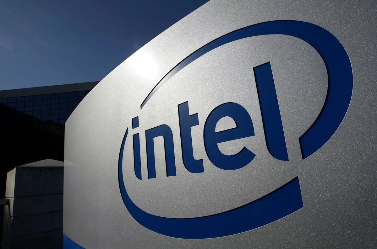
Intel’s (INTC) efforts to revive the chip big to its former glory might hinge on a brand new manufacturing course of the corporate calls 18A.
Quick for 18 angstroms — an angstrom is the same as 0.1 nanometers — 18A is, in keeping with Wall Road analysts and chip business consultants, Intel’s final hope to take again the semiconductor crown from rival TSMC (TSM).
Out there later this yr, 18A takes benefit of two manufacturing strategies that TSMC is not utilizing but: gate-all-around transistors and bottom energy. Intel says the applied sciences will enhance its chips’ efficiency and effectivity.
However Intel is not simply utilizing 18A to reclaim its place as a number one chipmaker. The corporate can be banking on utilizing the know-how to maneuver in on TSMC’s contract manufacturing enterprise by constructing 18A-based chips for itself and customized variations for third-party prospects.
However that’ll show troublesome. TSMC already builds chips for firms together with AMD, Apple, and Nvidia. Intel opened up its manufacturing enterprise to outdoors purchasers in 2021 beneath former CEO Pat Gelsinger. However Wall Road analysts and executives grew exasperated together with his technique and what they noticed as unrealistic targets for the enterprise, which misplaced $13.4 billion in 2024 regardless of recording a income of $17.5 billion.
Thus far, Amazon and Microsoft have signed on to construct their very own chips utilizing Intel’s 18A course of, with the hope that others will observe swimsuit. However CFO David Zinsner says third-party commitments are “not vital” but, in keeping with Reuters.
Intel’s 18A is so essential as a result of it is introducing two applied sciences to the corporate’s chips without delay. First, it is benefiting from gate-all-around transistors — next-generation transistors that may extra actively management the circulation of electrical energy by way of a chip. It is also utilizing a method known as bottom energy, which modifications the place and the way energy is delivered to a chip’s transistors to allow extra effectivity and higher efficiency.
Collectively, the 2 applied sciences would assist enhance AI software efficiency with out operating into vitality constraints, UC Santa Barbara engineering professor Kaustav Banerjee instructed Yahoo Finance. That will minimize down on issues like overheating — one thing that reportedly plagued Nvidia’s Blackwell graphics processing models (GPUs) once they had been in growth.
Taking first-mover benefit within the chip business sometimes means huge wins for a semiconductor producer. Intel’s founders invented trendy semiconductors, and the chipmaker was the primary to efficiently manufacture a brand new form of transistor known as Finfet in 2011.
Intel CEO Lip-Bu Tan seems at an occasion organized by the corporate in San Jose, Calif. (Andrej Sokolow/image alliance by way of Getty Photographs) ·image alliance by way of Getty Photographs
However TSMC flipped the script in 2019 when it turned the primary to efficiently use superior chipmaking know-how known as EUV lithography — large machines value a whole lot of tens of millions of {dollars} — to make semiconductors, which helped it soar previous Intel and make the world’s most superior AI chips for firms together with Apple and Nvidia.
That is not all. Intel additionally already needed to delay the rollout of 18A from the primary half of 2025 to the second half, in keeping with the corporate’s earlier earnings calls.
Attempting to good each bottom energy and gate-all-around transistors without delay introduces larger manufacturing complexity and larger room for error.
“Each of those applied sciences [are] enormously advanced on [their] personal,” Chris Miller, writer of “Chip Warfare,” instructed Yahoo Finance. “So it is even more durable to do them concurrently.”
A producing worker at Intel’s foundry in Oregon instructed Yahoo Finance on the situation of anonymity that the know-how wasn’t prepared for exterior prospects in December. In a follow-up interview in March, nonetheless, they stated 18A “has gotten quite a bit higher” and Intel staffers are “optimistic” about it.
One other manufacturing worker on the fab stated 18A is “on observe.” Nonetheless, they anxious that Intel’s deliberate layoffs may depress morale and hinder their work towards getting the method out the door.
TSMC is not sitting idly by, although. The corporate can be launching gate-all-around transistors by way of its N2 know-how, which it plans to launch later this yr. It is also working so as to add bottom energy to its chips in 2026.
Making certain 18A works is simply a part of the equation. Intel additionally has to show it will possibly enroll prospects to benefit from the know-how for their very own chips and might pump them out within the volumes they want.
“Can they do it? Sure, they will do it,” Financial institution of America analyst Vivek Arya stated. “However can they do it with the form of yield and scale like TSMC? That, I feel, stays to be seen.”
Gelsinger staked a part of Intel’s revival on his plans to show the corporate right into a third-party foundry. Tan seems to be set to stay to that plan. And whereas Intel expects its foundry enterprise, which has been hemorrhaging cash, to interrupt even by 2027, Wall Road is probably not prepared to attend that lengthy.
Varied analysts have known as for Intel to ditch its third-party foundry, and even get out of the chip manufacturing enterprise totally, and keep on with designing semiconductors like rivals AMD and Nvidia.
However since Intel is the US’s sole large-scale superior chip producer, the federal government is eager on protecting its manufacturing arm intact. Intel has secured $7.8 billion in US CHIPS Act funding, and ditching its foundry would put that funding in danger.
“The US does not need to be completely depending on international companies for superior manufacturing and R&D. Proper now, Intel is the one agency with superior R&D in the USA,” writer Chris Miller defined.
Whereas TSMC is increasing its US footprint, investing $165 billion in new crops and analysis services within the coming yr, solely one-third of its most superior chipmaking will happen within the US, the corporate stated in an April name with traders.
Nonetheless, Financial institution of America’s Vivek Arya stated TSMC’s US growth “blunts Intel’s benefit to some extent.”
For Intel, all of it comes all the way down to proving 18A can succeed. We’ll discover out later this yr.
Join Yahoo Finance’s Week in Tech e-newsletter. ·yahoofinance
Laura Bratton is a reporter for Yahoo Finance. Comply with her on Bluesky @laurabratton.bsky.social. E-mail her at laura.bratton@yahooinc.com.
E-mail Daniel Howley at dhowley@yahoofinance.com. Comply with him on X/Twitter at @DanielHowley.
For the newest earnings reviews and evaluation, earnings whispers and expectations, and firm earnings information, click on right here
Learn the newest monetary and enterprise information from Yahoo Finance